Home

Saturday, April 3, 2010

Overclock Your Nintendo Ds Lite

Why would you want to change the speed of your DS? Unlike regular computers and some other game systems like the PSP, DS (and GBA) games always expect the handheld to run at exactly the same speed. When you speed up or slow down the clock, the game speeds up or slows down. This is great for making your games harder or easier. It's also useful for squeezing some extra clock cycles out of the hardware so you can make more powerful homebrew apps. You can also show off how L33T you are to your friends if you are into that sort of thing (or if they even care).

What you need:


Take the DS Lite Apart
Turn the DS Lite upside down. Use a phillips screwdriver to remove the battery cover.

Remove the battery.

Remove the stylus.

Remove the GBA cartridge hole plugger thingy.

Battery Removed


Use a phillips and a tri-wing screwdriver to remove the eight screws from the back of the DS. Note: two of the screws are hidden under stick-on rubber feet. Use a utility knife to carefully peel them off so you can access the screws underneath. Try to set the feet somewhere where they'll stay sticky.

Put the screws in your parts container or you will never see them again.

Rear Cover Screws


Lift the back cover off of the DS. The bottom edge may need a little prying, but it should just snap apart.

Carefully remove the L and R buttons if they haven't popped off and fallen on the floor yet. Be careful when doing this; the pin and spring in these buttons fall out very easily and are easy to lose. Put them in your parts container when you find them.

Rear Cover Removed


There should be one screw left holding the PCB in place. Remove it.

PCB Screw


Disconnect the black antenna wire from the RF module and pull it out from under the game slot assembly.

Disconnect the white microphone wire from the PCB near the RF module and bend it out of the way.

Antenna and Microphone Connectors


Disconnect the small ribbon cable from the connector near the RF module. Do this by flipping the black part of the connector up and sliding the ribbon out.

Small Ribbon Connector


Flip the PCB and LCD screen together up out of the case. They will hinge on the ribbon cable that goes to the top screen.

Board and Screen Removed


Disconnect the remaining two ribbon cables. Do this by flipping the dark-grey part of the connectors up and sliding the ribbon out.

Large Ribbon 1


Large Ribbon 2


Place the LCD touch screen back in the case and set them aside. Now you have the PCB separate from the rest of the DS so you can work on it.

Pull straight up on the RF module until it comes free of the PCB. Set it aside.

RF Module Removed


Remove the Existing Crystal
There are four metal tabs that hold the game slot assembly onto the PCB. Desolder these. Solder wick is probably the easiest, but use whatever solder kung-fu works for you.

Desolder Slot Assembly


Lift up on the slot assembly. It will swing back on the pins which are still attached to the PCB. Now you have easy access to cryxtal X1.

Crystal X1


Desolder and remove the crystal. If you mangle it that's okay since you won't ever need it again.

Crystal X1 Removed


Attach a wire to one of the solder pads where the crystal used to be. This diagram shows you exactly which one:

CLK Connection


Bend the slot assembly back into place and re-solder it to the PCB.


Install the GBAccelerator DS
Flip the PCB over so that the front side is facing up.

Solder the three button wires (blue in diagram) and the LED wire (green in diagram) to their respective solder points. Route the wires across the board as shown in the diagram. This is important so that they don't interfere with any buttons, standoffs, etc. Let them hang off the edge for now.

GBAccelerator DS Lite Front Connections
LEDGreen
BUTTONP02
BUTTONP08
BUTTONP09


Diagram (Front)


Front Wiring


Lay the board next to the top half of the case.

Reconnect the ribbon cable that goes to the top screen. Note: the ribbon connectors in the DS Lite don't slide back together very easily. Make sure you slide the ribbon all the way in before flipping the latch back down or DS won't even boot.

Reconnect Large Ribbon 1


Lay the LCD touch screen on the PCB and reconnect its ribbon cable.

Reconnect Large Ribbon 2


Flip the LCD/PCB combo over into the top half of the case. Make sure the screen lines up with its opening. As you lower the board into position the tuft of wires you connected to the other side of the board should bend up and around the edge of the PCB.

Reconnect the small ribbon cable and the white microphone wire.

Replace PCB


Replace the screw that held the PCB into the top half of the case.

Use double-sided tape to stick the GBAccelerator DS chip to the PCB. Make sure you place it in the position shown or there might not be enough room for it when you go to put the bottom of the case back on.

Chip Placement


Make the remaining wiring connections as shown in the diagram. Be careful not to hold the soldering iron on any connection for too long or you could lift the pad from the DSAccelerator or DS board.

GBAccelerator DS Lite Back Connections
GNDGBA cartridge slot pin 32
V+GBA cartridge slot pin 1
CLKSolder pad where xtal used to be


Diagram (Back)


Once you are done you will (or at least should) end up with something that looks like this:

Installed 1


Installed 2


If your installation looks different, go fix it!


Put the DS Lite Back Together
Now you need to make a little extra room in the back cover for the chip you just added. Remove the three screws that hold the stylus channel onto the back cover.

Stylus Channel Screws


Remove the stylus channel. Use a utility knife to trim off the middle screw tab (the one that had the red arrow pointing to it).

Re-install the channel, but remember now you only need two screws. Save the third one for your next project.

Screw Tab Removed


Reinstall the RF module onto the DS Lite PCB.

Run the black antenna wire back under the slot assembly and connect it to the RF module.

Very carefully put the L and R buttons (including their pins and springs) back into place.

Reassembly


Gently lower the back cover onto the rest of the DS Lite. It should sit back down into position without requiring much force. If it feels like something is hitting the GBAccelerator chip, use needle-nose pliers to gently scoot the chip around until it is out of the way.

Replace the remaining screws that hold the back cover on.

Replace the two rubber feet that you had to remove.

Reinstall the battery.

Reinstall the battery cover.

(You probably want to leave the stylus and cartridge-plugger thing out so you can play.)

Flip the handheld over, put a game in and open the screen because it's time to test out your handiwork!


Testing Out Your Handiwork
Turn on the DS Lite. It should boot just like you hadn't spent the last hour or ten modifying it.

Start whatever game you inserted. It should look pretty normal too.

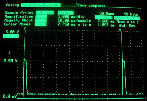
Press L, R and Select. Your game should start running faster now, and the power LED should start blinking to indicate that you are in "fast" mode (1.4x).

Press L, R and Select again. The game will go even faster and the LED will double-blink to let you know that you are in "ultra" mode (1.8x).

Press the buttons again. Now your game will be running much slower and the LED will be fading in and out ("slow-motion" mode, .66x)

One more press of the magic button combination will bring you back to normal, boring 1x.

Congratulations, you now have an overclocked Nintendo DS Lite! You even have a part left over, which is usually a good sign that you did a project right.

Credits to: N-Ds Mods

Tuesday, March 30, 2010

iPhone Stand from Spoon and Fork


Tools i use:

2Teaspoon and 3Fork
Aluminum Tape
Scissor as usual

Do it on your own risk bwahahahaha:D

The creator

Sunday, March 28, 2010

PSP 1000 Moddings USB charging By: Wesley


First disassemble your PSP all the way down to the motherboard, and remove the motherboard, here's a nice start...


Once you have removed the motherboard from the PSP turn it over. Here's the area on the motherboard you'll be working with...


The first point you will need to solder is at the USB port. Fitting the wire into the tight areas around the USB port is easier if you bend your wire a little so that it travels between some of the other components on the motherboard (as you can see above). Here's the solder point at the USB connector...


Next you will need to solder the wire to the power connector. Here's the solder point for the power connector...


Now let's test it out! Put your motherboard back into the PSP, hook up your power board, and insert the battery. Now hook up your USB cable like you normally would for data transfer, now look at your Power LED. Did it light up Orange like it does when your PSP is charging? If so then then that means that your new mod works!


Here you can see there's no battery in and no power plug, just the USB, and it's on and running...

Now put your PSP back together and enjoy it's new charging capability! You can also continue on to the companion tutorial for this mod, and convert your AC Adapter to a USB Charger!

Acer Laptop Service Manuals and FRU Documentation

If you are looking for Acer laptop service manuals, you can download them here. The site is in Russian but all links are in English.

You’ll find service manuals and FRU documentation for the following laptops:
1. Acer Aspire 1610 Series [ 4.5 Mb ]
2. Acer Aspire 3680 / 5570 / 5580 [ 4.6 Mb ]
3. Acer Aspire 4930 / 4930G Series [ 4.8 Mb ]
4. Acer Aspire 5050 / 3050 Series [ 11.7 Mb ]
5. Acer Aspire 5110 / 5100 / 3100 [ 7.0 Mb ]
6. Acer Aspire 5520 / 5220 Series [ 3.5 Mb ]
7. Acer Aspire 5530 / 5530G Series [ 7.4 Mb ]
8. Acer Aspire 5680 / 5630 / 3690 / Acer TravelMate 4280 / 4230 / 2490 [ 7.7 Mb ]
9. Acer Aspire 5710 / 5710G / 5310 / 5310G [ 3.2 Mb ]
10. Acer Aspire 5720 / 5720G [ 3.4 Mb ]
11. Acer Aspire 5920G [ 4.0 Mb ]
12. Acer Aspire 5930 / 5930Z / 5730Z Series [ 28.6 Mb ]
13. Acer Aspire 6920 [ 18.9 Mb ]
14. Acer Aspire 6930 / 6930G [ 8.8 Mb ]
15. Acer Aspire 6935 Series [ 23.2 Mb ]
16. Acer Aspire 7520 / 7220 Series [ 3.7 Mb ]
17. Acer Aspire 7720 / 7720G [ 3.4 Mb ]
18. Acer Aspire 7730 / 7730G [ 7.1 Mb ]
19. Acer Aspire 9420 / 9410 / 7110 / Acer TravelMate 5620 / 5610 / 5110 [ 9.1 Mb ]
20. Acer Aspire 9920 [ 6.6 Mb ]
21. Acer Ferrari 3000SG [ 3.4 Mb ]
22. Acer Ferrari 4000 [ 4.7 Mb ]
23. Acer TravelMate 2410 [ 2.7 Mb ]
24. Acer TravelMate 4070 / 4080 [ 3.9 Mb ]
25. Acer TravelMate 4210 / 4270 / 4670 / Acer Aspire 5620 / 5670 [ 6.2 Mb ]
26. Acer TravelMate 4220 / 2480 / Acer Aspire 5600 [ 20.7 Mb ]
27. Acer TravelMate 540 Series [ 7.0 Mb ]
28. Acer TravelMate 5720 / 5320 / Acer Extensa 5620 / 5220 [ 29.3 Mb ]
29. Acer TravelMate 5730 / Acer Extensa 5630 Series [ 23.4 Mb ]
30. Acer TravelMate 5710 / 5310 / Acer Extensa 5610 / 5210 [ 29.1 Mb ]
31. Acer TravelMate 7720 / 7320 [ 37.7 Mb ]
32. Acer Travelmate 7730 / 7730g [ 8.3 Mb ]
33. Acer TravelMate 8100 [ 4.5 Mb ]
34. Acer TravelMate 240 / 250 [ 5.1 Mb ]
35. Acer Aspire 4720 / 4720G / 4720Z / 4320 [ 3.1 Mb ]
36. Acer Aspire серии 4720Z / 4720 / 4320 Руководство Пользователя [ 3.4 Mb ]
37. Схема на ноутбук Acer Aspire 4720Z (Z01)-E3C [ 0.9 Mb ]
38. Acer Aspire 8935G [ 10.5 Mb ]
39. Acer Aspire 5110 / 5100 / 3100 / TravelMate 5510 / 5210 / Extens 5410 / 5010 [ 14.0 Mb ]
40. Acer Aspire 9300 / 7000 / Acer TravelMate 7510 [ 9.7 Mb ]
41. Acer Aspire 6530 [ 3.8 Mb ]
42. Acer Aspire 4520 / 4220 / 4520G / 4220G [ 9.1 Mb ]
43. Acer Aspire 5738G / 5738ZG / 5738Z / 5738 / 5338 / 5536 / 5536G / 5236 [ 19.4 Mb ]
44. Acer Aspire 2930 [ 10.4 Mb ]
45. Acer TravelMate 4
20 [ 8.9 Mb ]
46. Acer TravelMate 6492 [ 4.4 Mb ]
47. Acer TravelMate 3000 [ 4.7 Mb ]
48. Acer Aspire 4920 / 4920G [ 4.8 Mb ]
49. Acer TravelMate 4530 [ 6.8 Mb ]
50. Acer Aspire 4715z / 4315 [ 26 Mb ]
51. Acer TravelMate 2480 / 3260 / 3270 [ 4.7 Mb ]

IBM ThinkPad Computer hardware Maintenance manuals

HMM will provide you instructions for troubleshooting, diagnostics, removal and replacement laptop hardware. All IBM HMMs are publicly available. You can find HMM for your laptop on the IBM website or you can follow the link below. All HMMs are in pdf format, so you can download them and use at your convenience. For hardware replacement instructions find “Removing and replacing a FRU” chapter.

IBM ThinkPad Computer Hardware Maintenance Manuals Year 2001-2006
IBM ThinkPad A2*m, A2*p
IBM ThinkPad A2*e
IBM ThinkPad A21e
IBM ThinkPad A22* (Wireless models)
IBM ThinkPad A30, A30p, A31, A31p
IBM ThinkPad G40, G41
IBM ThinkPad R30, R31
IBM ThinkPad R32
IBM ThinkPad R40, R40e
IBM ThinkPad R50/p, R51
IBM ThinkPad R50e, R51e, R52
IBM ThinkPad R60, R60e
IBM ThinkPad T20, T21, T22, T23
IBM ThinkPad T30
IBM ThinkPad T40/p, T41/p, T42/p
IBM ThinkPad T43
IBM ThinkPad T43/p
IBM ThinkPad T60, T60p
IBM ThinkPad X20, X21, X22, X23, X24
IBM ThinkPad X30, X31, X32
IBM ThinkPad X40
IBM ThinkPad X41
IBM ThinkPad X41 Tablet
IBM ThinkPad X60/s
IBM ThinkPad Z60m
IBM ThinkPad Z60t
IBM ThinkPad Z61e, Z61m
IBM ThinkPad Z61t
IBM ThinkPad Computer Hardware Maintenance Manuals Year 1997-2001
TransNote
i Series 1200, 1300, ThinkPad 130
i Series 1400, 1500
i Series 1400, 1500
IBM ThinkPad 240
IBM ThinkPad 240X
IBM ThinkPad 380, 385, 560, 760, 765
IBM ThinkPad 380XD/385XD
IBM ThinkPad 380Z
IBM ThinkPad 390
IBM ThinkPad 390E
IBM ThinkPad 390X
IBM ThinkPad 560X
IBM ThinkPad 560Z
IBM ThinkPad 570/E
IBM ThinkPad 600
IBM ThinkPad 600X
IBM ThinkPad 770

Get IBM laptop manuals here: IBM ThinkPad notebooks hardware maintenance manuals

HP Compaq laptops manuals with disassembly instructions

Fixing a HP/Compaq laptop yourself? Need some help with taking the laptop apart? Here are links to manuals with step-by-step disassembly instructions. All these manuals are available from the HP website.
Here’s how to get the manual:
1. Follow the link
2. Select your model
3. Go to manuals
4. Find the maintenance and service guide and open it up (pdf file, some of them are huge)
5. Go to Removal and Replacement procedures chapter, you’ll find disassembly instructions in there
Manuals for the following Compaq Armada Notebook PC series. Get maintenance and service guide.
Compaq Armada 110, Compaq Armada 110s, Compaq Armada 1100, Compaq Armada 1500, Compaq Armada 1500c, Compaq Armada 1700, Compaq Armada 1750, Compaq Armada 3500, Compaq Armada 4100, Compaq Armada 4200, Compaq Armada 6500, Armada 7300, Compaq rmada 7400, Compaq Armada 7700, Compaq Armada 7800, Compaq Armada e500, Compaq Armada e500s, Compaq Armada E700, Compaq Armada m300, Compaq Armada m700, Compaq Armada SB, Compaq Armada V300
Manuals for the following Compaq Evo Notebook PC series. Get maintenance and service guide.
Compaq Evo n150, Compaq Evo n160, Compaq Evo n180, Compaq Evo n400c, Compaq Evo n410c, Compaq Evo n600c, Compaq Evo n610c, Compaq Evo n610v, Compaq Evo n620c, Compaq Evo n800c, Compaq Evo n800v, Compaq Evo n800w, Compaq Evo n1000c, Compaq Evo n1000v, Compaq Evo n1005v, Compaq Evo n1010v, Compaq Evo n1015v, Compaq Evo n1020v, Compaq Evo n1050v, Compaq Evo n200, Compaq Evo n110, Compaq vo n115
Manuals for the following HP Compaq Notebook PC series. Get maintenance and service guide.
HP Compaq 2400, HP Compaq 4400, HP Compaq 6100, HP Compaq 6200, HP Compaq 6300, HP Compaq 6305, HP Compaq 7400, HP Compaq 8200, HP Compaq 8400, HP Compaq 9400, HP Compaq nc4000, HP Compaq nc4010, HP Compaq nc4200, HP Compaq nc6000, HP Compaq nc6400, HP Compaq nc8000, HP Compaq nw8000, HP Compaq nw8240, HP Compaq nx4300, HP Compaq nx4800, HP Compaq nx4820, HP Compaq nx5000, HP Compaq nx6130, HP Compaq nx7000, HP Compaq nx7010, HP Compaq nx7100, HP Compaq nx7200, HP Compaq nx7220, HP Compaq nx7300, HP Compaq nx9000, HP Compaq nx9005, HP Compaq nx9008, HP Compaq nx9010, HP Compaq nx9020, HP Compaq nx9030, HP Compaq nx9040, HP Compaq nx9100, HP Compaq nx9105, HP Compaq nx9110, HP Compaq nx9500, HP Compaq nx9500A, HP Compaq nx9600
Manuals for the following HP Pavilion Notebook PC series. Get maintenance and service guide.
HP Pavilion de2000, HP Pavilion dv1000, HP Pavilion dv2000, HP Pavilion dv4000, HP Pavilion dv5000, HP Pavilion dv6000, HP Pavilion dv8000m, HP Pavilion dv9000, HP Pavilion n Notebook PC series, HP Pavilion tx1000, HP Pavilion xf Notebook PC series, HP Pavilion xh Notebook PC series, HP Pavilion xt Notebook PC series, HP Pavilion xu Notebook PC series, HP Pavilion xz Notebook PC series, HP Pavilion zd7000, HP Pavilion zd8000, HP Pavilion ze1000, HP Pavilion ze2000, HP Pavilion ze4000, HP Pavilion ze5000, HP Pavilion zt1000, HP Pavilion zt3000, HP Pavilion zu1000, HP Pavilion zv5000, HP Pavilion zv6000, HP Pavilion zx5000
Manuals for the following HP Presario Notebook PC series. Get maintenance and service guide.
Compaq Presario 300, Compaq Presario 700, Compaq Presario 800, Compaq Presario 900, Compaq Presario 1000, Compaq Presario 1100, Compaq Presario 1200, Compaq Presario 1400, Compaq Presario 1500, Compaq Presario 1600, Compaq Presario 1700, Compaq Presario 1800, Compaq Presario 1900, Compaq Presario 2100, Compaq Presario 2200, Compaq Presario 2500, Compaq Presario 2700, Compaq Presario 2800, Compaq Presario 3000, Compaq Presario B1000, Compaq Presario B2000, Compaq Presario B3000, Compaq Presario C300, Compaq Presario C500, Compaq Presario F500, Compaq Presario M2000, Compaq Presario R3000, Compaq Presario R4000, Compaq Presario V1000, Compaq Presario V2000, Compaq Presario V3000, Compaq Presario V4000, Compaq Presario V5000, Compaq Presario V6000, Compaq Presario X1000, Compaq Presario X1100, Compaq Presario X1200, Compaq Presario X1300, Compaq Presario X1400, Presario X1500, Compaq Presario X6000
Manuals for the following HP Special Edition Notebook PCs. Get maintenance and service guide.
Special Edition L2000 CTO Notebook PC, Special Edition L2005A3, Special Edition L2005A4, Special Edition L2005CL, Special Edition L2005CM, Special Edition L2005CO, Special Edition L2005CU, Special Edition L2005CX, Special Edition L2005US, Special Edition L2098XX, Special Edition L2099XX, Special Edition L2105CA, Special Edition L2105CL, Special Edition L2105NR, Special Edition L2205NR, Special Edition L2300 CTO Notebook PC, Special Edition L2310CU

Saturday, March 27, 2010

Set PS1 Controller as PSP Controller by ACIDMODS

Soldering to the Powerboard

For the X [] /\ and O buttons, I found it easiest to solder through the vias on the powerboard. If you use 30awg wire you can run the wires under the board and poke the wire up through the holes, then just apply a little solder and trim away any excess wire. For the button bar connections it is similar, except these are blind vias, so you have to go through the top.


The picture below shows the connector pinout for the cable that links the powerboard and motherboard. A good solder point for the right trigger button can be found at one end of this connector, as well as alternative points for the other powerboard connections.


Soldering to the D-pad

I use a cheap ($15 at RadioShack) "helping hands" soldering clamp that is very useful for this type of precise work. It has a set of gator clips and a magnifying glass on adjustable arms, plus a soldering iron holder that I continually burn myself on.

To begin, clean the pins on the back of the connector with some rubbing alcohol. Next apply a little flux to the pins you are going to be soldering to. Because the pins are so small and close together, I decided not to add any solder to them directly, as it is very easy to bridge them with excess solder. So for each of the five points this was the basic procedure:

•   Strip a short amount at the end of the wire
•   Dip the stripped end in flux
•   Melt a small amount of solder onto iron tip
•   Touch the tip of the wire to the iron to transfer a small amount of solder
•   Dip tinned wire end back into flux again
•   Clean all excess solder f-rom iron tip
•   Hold the wire firmly in place against connector pin with tweezers
•   Carefully touch iron tip to the back of the wire (the flux on the wire and pin should help the solder bond quickly with the pin)
•   Hold the wire very still for a couple seconds while the solder cools
•   Inspect under magnification to ensure there is a good bond and no bridged pins

Once all the wires are soldered its a good idea to check everything again with a multimeter, then adjust your wires so they will not interfere with the fit of other components (picture 2). I applied a little superglue to the wires to secure them to each other and keep them in shape.


Soldering to the Power Switch

This may be useful if you have a broken power switch and want to send the On/Off/Standby and Hold functions out to an external controller or switch. The switch basically works like the other buttons and activates these functions by grounding pins 1, 3, or 4 to pin 2. The power on/off and standby functions are all activated by pin 4 when grounded to pin 2 (power off or standby is determined by how long the switch is held in position.)


Analog Stick Contacts

The joystick contacts on the motherboard can be wired to external potentiometers to provide analog input. If you aren't familiar with how this type of potentiometer based joystick works, here is a basic summary.

Potentiometers are variable resistors, inside them is a resistive material with three pins connected to it. On either end of the resistive material are the power and ground pins, these typically remain at a constant voltage. The third pin is called the wiper, this is just a piece of metal that can move along the resistive material (in this case the wiper is attached to the arm of the joystick). As the wiper moves closer to ground the voltage read from this pin approaches 0, as it moves closer to the power input the wiper voltage approaches whatever the supply voltage is. When the wiper is directly in the middle, its voltage will be half of the input voltage (in accordance with Ohm's law). By reading the voltage on the wiper pin, the psp is able to determine the position of the joystick at any time.

Two different examples for providing analog input are shown in this post, one using an MCP4251 digital potentiometer, and another using hardwired Ps1 controller joysticks. When looking at your PSP motherboard in the way it would normally be oriented while using the PSP, the analog connections are as follows:

  [[ ]  ]  =GND
[  [ ]]    =X-Axis
  [[ ]]    =+2.5v
[  [ ]]    =Y-Axis

The 2.5v supply to the joystick is not constant, but pulsed for approximately 200µs at 130Hz, this can be seen in the oscilloscope view below. These 2.5v pulses are only present when the running application requires input from the joystick, otherwise the joystick supply will be at a constant 0v.


Using a Microcontroller to Interface a Ps1/Ps2 controller to the PSP

The following code written for the ATmega168 microcontroller (should also work with the mega48 and 88) allows a Ps1/Ps2 controller to be used to control a PSP through wires soldered to the points shown in the images above. An MCP4251 digital potentiometer is also used to provide analog input. The benefit to this approach is that any Ps1/Ps2 controller can be used without having to modify the controller in any way, so wireless controllers can also be used. I still need to draw up a connection schematic and write a proper description of this, but for now here is the code.

Code: [Select]
/* MCP4251 8-bit SPI digital potentiometer, ATmega168 *-bit microcontroller */

#include
#define F_CPU 8000000UL
#include
#include
#include

#define LED_PORT      PORTC   // port, data direction, and input register definitions
#define LED_DDR         DDRC
#define ATTENTION_PORT      PORTC
#define   ATTENTION_DDR      DDRC
#define CS_PORT         PORTC
#define CS_DDR         DDRC
#define BUTTON0_PIN      PIND

#define PSP_CROSS      PC1   // I/O pin definitions
#define   PSP_SQUARE      PC2
#define   PSP_TRIANGLE      PD2
#define   PSP_CIRCLE      PD3
#define   PSP_UP         PD4
#define PSP_DOWN      PD5
#define PSP_LEFT      PD6
#define PSP_RIGHT      PD7
#define PSP_START      PB0
#define PSP_SELECT      PB1
#define PSP_HOME      PB6
#define PSP_L1         PB7
#define PSP_R1         PC0
#define   STATUS_LED_GREEN   PC5   // green LED cathode on PC5; indicates psx controller connected
#define COMMAND         PB3   // SPI MOSI; sends commands f-rom AVR to DSC
#define DATA         PB4   // SPI MISO; receives incoming data f-rom DSC; 1k external pull-up resistor required
#define CLOCK         PB5   // SPI SCK; serial clock controlled by AVR, DATA is read on rising edge
#define ATTENTION      PC3   // initiates and closes each data packet transmission
#define   CS         PC4   // chip select for MCP4251
#define SS         PB2   // SPI slave select pin; set as output to ensure AVR remains SPI master
#define BUTTON0         PD1   // button to connect/disconnect potentiometer terminals within the MCP4251

#define   PS_SELECT      0   // psx_data[0] byte
#define   PS_L3         1
#define   PS_R3         2
#define   PS_START      3
#define   PS_UP         4
#define   PS_RIGHT      5
#define   PS_DOWN         6
#define   PS_LEFT         7

#define   PS_L2         0   // psx_data[1] byte
#define   PS_R2         1
#define   PS_L1         2
#define   PS_R1         3
#define   PS_TRIANGLE      4
#define   PS_CIRCLE      5
#define   PS_CROSS      6
#define   PS_SQUARE      7

#define Y_POT_ADDRESS      0x00   // MCP4251 wiper 0 register address (datasheet p.48)
#define X_POT_ADDRESS      0x10   // MCP4251 wiper 1 register address (datasheet p.48)
#define TCON_ADDRESS      0x40   // MCP4251 terminal control register (datasheet p.35)
#define TCON_CONNECT_ALL   0xFF   // connect all six potentiometer terminals within the MCP4251 (datasheet p.36)
#define TCON_DISCONNECT_ALL   0x88   // disconnect all six potentiometer terminals within the MCP4251 (datasheet p.36)

/* SR0 (status register 0) bit defines */
#define   DSC_CONNECT_STATUS_BIT   0
#define TCON_CONNECT_STATUS_BIT   1
#define BUTTON0_STATUS_BIT   2

//SPE enables SPI hardware; DORD sets data order to LSB first; MSTR selects master mode; CPOL sets clock polarity (high when idle)
//CPHA selects data setup on leading (falling) edge of clock, read on trailing (rising) edge; SPR1, SPI2X sets clock frequency prescale factor at 32 (250kHz clock)
#define PSX_SPI_CONFIG      SPCR = 0x7E;\
            SPSR |= _BV(SPI2X);
 
//SPE enables SPI hardware; DORD low sets data order to MSB first; MSTR selects master mode; CPOL low sets clock polarity (low when idle)
//CPHA low selects data setup on trailing (falling) edge of clock, read on leading (rising) edge; SPR1, SPI2X sets clock frequency prescale factor at 32 (250kHz clock)
#define MCP4251_SPI_CONFIG   SPCR = 0x52;\
            SPSR |= _BV(SPI2X);

// macro for mapping button presses f-rom psx controller to psp
#define MAP_DIGITAL_CONTROL(in_byte, in_bit, out_byte, out_bit){\
            (~in_byte & _BV(in_bit)) ? (out_byte &= ~_BV(out_bit)) : (out_byte |= _BV(out_bit));\
   }

/* init() sets all registers and enables necessary interrupts */
void init(void){

   /*Set pin I/O registers*/
   DDRB |= _BV(SS) | _BV(COMMAND) | _BV(CLOCK) | _BV(PSP_START) | _BV(PSP_SELECT) | _BV(PSP_HOME) | _BV(PSP_L1);
   DDRC |= _BV(STATUS_LED_GREEN) | _BV(ATTENTION) | _BV(CS) | _BV(PSP_R1) | _BV(PSP_CROSS) | _BV(PSP_SQUARE);
   DDRD |= _BV(PSP_TRIANGLE) | _BV(PSP_CIRCLE) | _BV(PSP_UP) | _BV(PSP_DOWN) | _BV(PSP_LEFT) | _BV(PSP_RIGHT);
 
   PORTD |= _BV(PSP_TRIANGLE) | _BV(PSP_CIRCLE) | _BV(PSP_UP) | _BV(PSP_DOWN) | _BV(PSP_LEFT) | _BV(PSP_RIGHT) | _BV(BUTTON0);
   PORTC |= _BV(STATUS_LED_GREEN) | _BV(ATTENTION) | _BV(CS) | _BV(PSP_R1) | _BV(PSP_CROSS) | _BV(PSP_SQUARE);
   PORTB |= _BV(SS) | _BV(COMMAND) | _BV(CLOCK) | _BV(PSP_START) | _BV(PSP_SELECT) | _BV(PSP_HOME) | _BV(PSP_L1);
}

/* Core AVR-DSC send/receive communication function; takes command_byte, returns single data byte f-rom controller. */
uint8_t psx_comm(uint8_t command_byte){

   SPDR = command_byte;         // Write command byte to SPI data register to begin transmission (pg. 175)
   while(!(SPSR & _BV(SPIF)));      // Conditional loop to prevent write collision
   _delay_us(30);            // Delay between byte transmissions
   return(SPDR);            // Return byte f-rom controller in shift register receive buffer (pg. 175)
}

/* AVR-MCP4251 write command plus data to MCP4251 register */
void write_mcp4251_reg(uint8_t register_address, uint8_t data){
 
   CS_PORT &= ~_BV(CS);      // lower MCP4251 chip select line
   _delay_us(2);         // delay required by datasheet
   SPDR = register_address;   // write first 8-bit command+address prefix
   while(!(SPSR & _BV(SPIF)));   // wait for transmission complete flag to set
   SPDR = data;         // write data for x-axis potentiometer
   while(!(SPSR & _BV(SPIF)));   // wait for transmission complete flag to set
   _delay_us(2);         // delay again for no good reason
   CS_PORT |= _BV(CS);      // return chip select line high
}

/* Functions for remapping buttons between controllers */
void OR_map(uint8_t source_byte, uint8_t destination_byte, uint8_t source_bit, uint8_t destination_bit){

   if(~source_byte & _BV(source_bit))
      destination_byte &= ~_BV(destination_bit);
   }

/* Function to simplify configuration of psx controller; requires 4 command bytes, loop_bytes sets number of bytes following the default 6 */
uint8_t config_comm(uint8_t byte2, uint8_t byte4, uint8_t byte5, uint8_t byte6, uint8_t loop_bytes){

   uint8_t config_id = 0x00;
   ATTENTION_PORT &= ~_BV(ATTENTION);
 
   _delay_us(16);

   psx_comm(0x01);
   config_id = psx_comm(byte2);
   psx_comm(0x00);
   psx_comm(byte4);
   psx_comm(byte5);
   psx_comm(byte6);

   for(uint8_t x = 0; x < loop_bytes; x++)
      psx_comm(0x00); 
     
   _delay_us(16);

   ATTENTION_PORT |= _BV(ATTENTION);
   return(config_id);
}

int main(void){

   uint8_t psx_data[6];         // array stores data f-rom psx controller
   uint8_t SR0 = 0x00;         // status register 0
   uint8_t   psx_config_counter = 0x00;   // counter to increment psx controller config sequence
   uint8_t psx_config_id = 0x00;      // mode ID given by psx controller, 0x41 = digital, 0x73 = analog
   uint8_t left_analog_x = 0x80;
   uint8_t left_analog_y = 0x80;
   uint8_t right_analog_x = 0x80;
   uint8_t right_analog_y = 0x80;
 
   init();                     // set important AVR configuration registers
   _delay_ms(200);
   MCP4251_SPI_CONFIG;               // configure AVR SPI registers for MCP4251 communication
   write_mcp4251_reg(TCON_ADDRESS, TCON_CONNECT_ALL);   // initialize MCP4251 by setting TCON to connect all potentiometer terminals internally
   SR0 |= _BV(TCON_CONNECT_STATUS_BIT);
   _delay_us(16);

   /* Infinite while loop*/
   while(1){

      psx_data[0] = 0xFF;      // reset data variables to inactive values
      psx_data[1] = 0xFF;
      left_analog_x = 0x80;
      left_analog_y = 0x80;
      right_analog_x = 0x80;
      right_analog_y = 0x80;

      PSX_SPI_CONFIG;         // configure AVR SPI registers for psx communication
      _delay_us(4);

      if(SR0 & _BV(DSC_CONNECT_STATUS_BIT)){         // test if a controller is connected and configured
         ATTENTION_PORT &= ~_BV(ATTENTION);      // begin communication with psx controller by lowering select line
         _delay_us(16);               // required delay between select line low and data transmission


         psx_comm(0x01);               // byte 0; standard controller address header
         psx_config_id = psx_comm(0x42);         // byte 1; standard polling command
                if(psx_comm(0x00) == 0x5A){              // byte 2; standard header, data reply should always be 0x5A, tests connection status

                 for(uint8_t x = 0; x < ((psx_config_id & 0x0F) << 1); x++)    // loop loads data array with mode specific byte count
                       psx_data[x] = psx_comm(0x00);
             
                 _delay_us(16);                      // delay following data transmission before ATTENTION returns high

                   ATTENTION_PORT |= _BV(ATTENTION);         // end communication with DSC
                 LED_PORT &= ~_BV(STATUS_LED_GREEN);       // green status LED on (controller connected)
       
            if(psx_config_id == 0x73){      // if psx controller is in analog mode...
                    right_analog_x = psx_data[2];   // copy x/y axis values f-rom joysticks into variables
               right_analog_y = psx_data[3];
               left_analog_x = psx_data[4];
               left_analog_y = psx_data[5];
                }
              }
              else{
                 SR0 &= ~_BV(DSC_CONNECT_STATUS_BIT);     // if 0x5A not received in command byte 2, controller != connected; set status register
                   LED_PORT |= _BV(STATUS_LED_GREEN);       // green status LED off (controller not connected)
              }
      }

          if(!(SR0 & _BV(DSC_CONNECT_STATUS_BIT))){
              // this switch handles the configuration commands to send over six main loops when the DSC is first plugged in
              switch(psx_config_counter){
                    case    0:    psx_config_id = config_comm(0x42, 0x00, 0x00, 0x00, 0x00); psx_config_counter = 1; break; // standard initial polling request, 5 bytes total
                     case    1:    psx_config_id = config_comm(0x43, 0x01, 0x00, 0x00, 0x00); psx_config_counter = 2; break; // enter config mode, 5 bytes total
                     case    2:    psx_config_id = config_comm(0x44, 0x01, 0x03, 0x00, 0x03); psx_config_counter = 3; break; // enable analog mode and lock controller, 9 bytes total
                     case    3:    psx_config_id = config_comm(0x4D, 0x00, 0x01, 0xFF, 0x03); psx_config_counter = 4; break; // vibration motor control byte mapping
                     case    4:    psx_config_id = config_comm(0x43, 0x00, 0x5A, 0x5A, 0x03); psx_config_counter = 5; break; // exit config mode
                    case    5:    psx_config_id = config_comm(0x42, 0x00, 0x00, 0x00, 0x03); SR0 |= _BV(DSC_CONNECT_STATUS_BIT); psx_config_counter = 0; break;
                  }
                 // test will reset configuration switch if a communication error occurs or controller is disconnected before full configuration is complete
              if((psx_config_id == 0x00) || (psx_config_id == 0xFF)){ psx_config_counter = 0; SR0 &= ~_BV(DSC_CONNECT_STATUS_BIT);}
          }

     
      MCP4251_SPI_CONFIG;               // configure AVR SPI registers for MCP4251 communication
      _delay_us(4);
      write_mcp4251_reg(X_POT_ADDRESS, left_analog_x);   // write value f-rom psx controller left analog x-axis to wiper 0 register in MCP4251
      _delay_us(2);
      write_mcp4251_reg(Y_POT_ADDRESS, left_analog_y);   // write value f-rom psx controller left analog y-axis to wiper 1 register in MCP4251
     
      MAP_DIGITAL_CONTROL(psx_data[0], PS_UP, PORTD, PSP_UP);      // map digital button presses f-rom psx controller to psp
      MAP_DIGITAL_CONTROL(psx_data[0], PS_DOWN, PORTD, PSP_DOWN);   // all buttons are active low
      MAP_DIGITAL_CONTROL(psx_data[0], PS_LEFT, PORTD, PSP_LEFT);
      MAP_DIGITAL_CONTROL(psx_data[0], PS_RIGHT, PORTD, PSP_RIGHT);
      MAP_DIGITAL_CONTROL(psx_data[0], PS_SELECT, PORTB, PSP_SELECT);
      MAP_DIGITAL_CONTROL(psx_data[0], PS_START, PORTB, PSP_START);
      MAP_DIGITAL_CONTROL(psx_data[0], PS_R3, PORTB, PSP_HOME);
      MAP_DIGITAL_CONTROL(psx_data[1], PS_CROSS, PORTC, PSP_CROSS);
      MAP_DIGITAL_CONTROL(psx_data[1], PS_SQUARE, PORTC, PSP_SQUARE);
      MAP_DIGITAL_CONTROL(psx_data[1], PS_TRIANGLE, PORTD, PSP_TRIANGLE);
      MAP_DIGITAL_CONTROL(psx_data[1], PS_CIRCLE, PORTD, PSP_CIRCLE);
      MAP_DIGITAL_CONTROL(psx_data[1], PS_R1, PORTC, PSP_R1);
      MAP_DIGITAL_CONTROL(psx_data[1], PS_L1, PORTB, PSP_L1);

      if(~psx_data[1] & _BV(PS_L2)){ (PORTD &= ~_BV(PSP_LEFT));}   // map secondary shoulder buttons to left/right directional buttons
      if(~psx_data[1] & _BV(PS_R2)){ (PORTD &= ~_BV(PSP_RIGHT));}
      if(right_analog_x > 178){ (PORTD &= ~_BV(PSP_CIRCLE));}      // define right analog dead zone and map movements to digital buttons
      else if(right_analog_x < 78){ (PORTC &= ~_BV(PSP_SQUARE));}
      if(right_analog_y > 178){ (PORTC &= ~_BV(PSP_CROSS));}
      else if(right_analog_y < 78){ (PORTD &= ~_BV(PSP_TRIANGLE));}

      // the following checks for a single press of button0 and toggles the connection of the potentiometer terminals within the MCP4251
          if(~BUTTON0_PIN & _BV(BUTTON0)){
              if(!(SR0 & _BV(BUTTON0_STATUS_BIT))){          // BUTTON0_STATUS_BIT indicates whether or not the button is already being pressed
                      if(SR0 & _BV(TCON_CONNECT_STATUS_BIT)){         // if poterntiometer terminals are already connected...
               write_mcp4251_reg(TCON_ADDRESS, TCON_DISCONNECT_ALL);
                             SR0 &= ~_BV(TCON_CONNECT_STATUS_BIT);   // ...disconnect potentiometer terminals and set status bit
            }
                      else if(!(SR0 & _BV(TCON_CONNECT_STATUS_BIT))){ // if poterntiometer terminals are already disconnected...
               write_mcp4251_reg(TCON_ADDRESS, TCON_CONNECT_ALL);
                             SR0 |= _BV(TCON_CONNECT_STATUS_BIT);    // ...connect potentiometer terminals and set status bit
            }
                 SR0 |= _BV(BUTTON0_STATUS_BIT);              // set BUTTON0_STATUS_BIT flag so we know the button press has been recognized
              }
          }

      if(BUTTON0_PIN & _BV(BUTTON0))               // if the button is high (default state)...
              SR0 &= ~_BV(BUTTON0_STATUS_BIT);         // ...reset BUTTON0_STATUS_BIT to wait for next press
     
   _delay_ms(15);            //delay for roughly 60 samples per second
     
   } // while(1)


} // main()


Hardwiring a Ps1 Controller

As an alternative to reading and interpreting data f-rom the controller, it can also be modified to act as a set of independent switches with parallel output. This will result in the controller no longer being usable as a playstation controller, so it is only recommended for controllers which are already defective. The following image shows the pinouts for rewiring a Sony SCPH-1200 Ps1 Analog Controller for a point to point connection to the PSP, with the addition of a modified right analog stick (A2D mod) to mimic the X, [], /\, and O buttons.


The Ps1 controller and the PSP differ slightly in the way the analog stick is grounded, so some simple modifications will need to be made to the controllers PCB for it to work. This may involve cutting traces, desoldering components, or bridging points with additional wires. It’s difficult to be specific here because Sony seems to change the PCB layouts on their controllers a lot. What is important is that the pins on the potentiometers (3 on each) are wired and grounded according to the diagrams above. Keep checking all of the pot pins with a multimeter, and make any necessary modifications until everything is correct.

The points labeled A1, A2, and A3 on the left analog stick will be wired to three of the four contacts on the PSPs Analog nub or the motherboards analog contact pads. The remaining contact should be grounded with the other buttons. So, when looking at your PSP motherboard in the way it would normally be oriented while using the PSP, the analog connections are as follows:

  [[ ]  ]  =GND
[  [ ]]    =X-Axis (A1)
  [[ ]]    =+2.5v  (A2)
[  [ ]]    =Y-Axis (A3)

The wiring of the right analog stick shown in the diagram is optional, and allows it to perform the same function as the “Razor Nub” on the PSP. This will require some additional work beyond just rewiring the solder points, to make the potentiometers function like simple momentary switches. You will need to desolder the right analog stick, remove the potentiometers, and cut away part of the conductive track inside them. This is all much easier than it sounds, and TimmyDX has made an excellent video tutorial on how to do it.

As I mentioned earlier there were many different hardware revisions to these controllers, so yours may not look exactly like the picture, but the basic ideas here should be applicable for most Ps1 analog controllers. I think it is safe to assume that the pin order on the ribbon cable connector should be the same for all Ps1 controllers which use the membrane button contacts, but I am not 100% sure of this. The early Ps1 Analog controllers have the button contacts on a solid PCB, in which case these pinouts do not apply.

Thursday, March 25, 2010

The Hack is Back: OS X Fixed To Run on Atom Netbooks

When Apple dropped support for Atom processors in OS X 10.6.2, effectively killing Hackintosh netbooks, we knew that somebody would fix things. We didn’t know that it would happen so fast.
Just over a week after the update, Russian hacker “Tea” has made a patched kernel specifically for the Atom CPU. Simply copying this to the root level of your drive and rebooting should make everything work just like it did in 10.6.1. Of course, if you are suffering the endless gray screen on boot that characterizes the problem OS, then you’ll somehow need to get into the hard drive from the outside, perhaps by booting from the DVD or USB stick you used to hack your Mac in the first place.
Tea himself didn’t actually test out this kernel (which is the very lowest level of the OS) on 10.6.2, but some brave (desperate?) folks at the Insanely Mac forums tried it and it apparently works fine.
My Wind Hackintosh is still running the previous version of OS X 10.5 Leopard. I see no reason to update it, especially with all these shenanigans.


1. Download zip to Desktop
2. Unzip by double click
3. Open Terminal.app
4. sudo -s
5. Enter your root password
6. cd /
7. mv mach_kernel mach_kernel_1062
8. cp ~/Desktop/mach_kernel /
9. chown 0:0 mach_kernel
10. reboot
Eeebox B202 with N270
Acer Aspire ONEZG5
Asus EeePC 1000HE
Toshiba NB205

Credits to: TeaBag

Abuse iPhone gets Polished to Perfection


The iPhone is a beautiful piece of hardware but a few months in your pocket along with those keys and coins is enough to scratch it up. Now, instead of toting a clawed-out piece of hardware, you can apply some elbow grease and restore it to near perfection
Hack n Mod has posted a cool tutorial on how to give an abused iPhone a fresh out-of-the-box look.
To fix scratches on the back,  you need to gently dry sand it, then add some water to wet sand and polish it with a 3M Headlight Lens Restoration Kit. The detailed step-by-step pictorial offers information on what grit of sandpaper to use and how to get the mirror-like finish.
The only catch is that the Apple logo at the back is erased in the process but that’s a small price to pay. And it’s not like anyone can mistake the iPhone for another phone–whether Apple’s logo is on there or not.
Fixing scratches on the display is a little more tricky because it involves getting a replacement top layer but that’s available on eBay for $10. Just follow the instructions to open up the front cover and its simple enough to do.
The technique doesn’t apply to just the iPhone. You can take any scratched-up phone and polish it to get a new look.